


LCD and OLED Display
Systems > LCD & OLED Displays
LCD and OLED Display Thin Film Transistor (TFT) Crystallization
Annealing, liquid and solid phase crystallization applications are of great importance for the preparation of silicon films for the production of large area electronics and semiconductor devices.
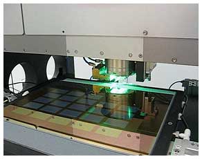
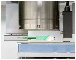
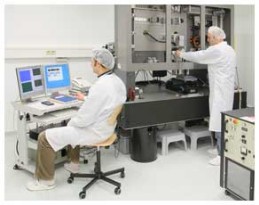
INNOVAVENT application lab exposure
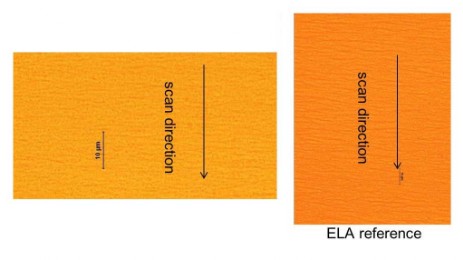
Microscope photo of a 50nm a-Si film after UV-SLA and ELA
LCD and OLED displays take advantage of the thin film transistor performance to switch the display pixel matrix. Driver electronics, memory and CPU circuits can be directly produced on the glass substrate. Thin silicon films are transferred into the liquid phase and controlled solidification results in homogenous crystallization providing high electron/hole mobility.
Thin film transistors (TFT) are built up in the p-Si film to switch the polarization in LCDs or to control the OLED current to generate the RGB picture.
The a-Si film electron mobility is enhanced by a factor of 500-1000 when generating the p-Si film from the a-Si. The green laser light is aborbed in a 50-70nm a-Si film (absorption coefficient ~200.000cm-1), however in p-Si 20x less (~5.000cm-1).
UV laser light of 343nm wavelength is well absorbed in a 10nm a-Si and p-Si layer (>1.000.000cm-1).
GLA (Green Laser Annealing) is applying pulsed 532/515nm laser pusles. UV-SLA (UV Solid State Laser Annealing) operates with 343nm. Both processes are economical and techical alternatives to the “near complete melt” ELA (Excimer laser annealing) of a-Si films. Laser pulse duration of 10-100ns is suitable to heat the a-Si film and keep the glass substrate at room temperature. Mechanical stress or thermal damage to the glass is avoided.
Prof James Im and coworkers from Columbia University published first results in the 90's (e.g. Robert S. Sposili, James S. Im, Sequential lateral solidification of thin silicon films on SiO2, Applied Physics Letters 69, p. 2864 (1996)) and several procedure patents were filed.
The GLA process fits well with LCD TFTs. The GLA process is a single pulse process. The green wavelength is absorbed in the fresh a-Si when scanning. The generated p-Si absorbes 20x less. The grain size distribution in the generated p-Si is sufficient for high resolution LCD TFTs. However, the variation in grain size and film roughness has not yet reached the requirements for OLED TFTs.
A 30µm FWHM Gaussian line up to 750mm length is created from fiber coupled 532nm pulsed (60-100ns) laser light. Very attractive is the low CoO (ca. 20% compared to excimer lasers, CoO = cost of ownership) and the minimum maintenance (availability of DPSSL >90%) compared to excimer laser annealing systems.
The 343nm UV-SLA process is very similar to the ELA process. The absorption in a-Si and p-Si is the same (as with 308nm). Multi shot absorption while scanning creates a uniform grain size distribution. The short pulse DPSSL (15-20ns) reduces the energy density to 200-250mJ/cm² compared to ~420mJ/cm² with excimer lasers. The flat top profile in the scan axis of 30-100µm width allows to create the ELA typical grain pattern with the wavelength period. UV-SLA provides the potential of enhanced uniform films through the small pitch of 1-2µm at 10kHz rep.-rate (20µm @ 600Hz for ELA) and this at higher throughput and reduced cost of ownership (40-50% of ELA).
A 500mm long line with a 30µm flat top can be created by multiplexing six TruMicro 7370 (20mJ, 10 kHz), 15-20ns) with an energy density of >250mJ/cm². Next generation UV-DPSSL need to provide >40mJ to create 750mm long lines with a 50µm flat top.
| Laser Optics for LCD and OLED Display | ||||