


Semiconductor Doping Activation Using Pulsed Green Laser Radiation
Systems > Semiconductor Processing
Semiconductor chips such as IGBTs and CMOS image sensors can perform their various functions due to the fact that different regions are doped with different kinds of dopants and thus different electrical characteristics are achieved. Doping is normally done by ion implantation. These implants have to be made electrically effective or to be “activated” by a thermal process. During this thermal process often temperature levels close to the melting point of the semiconductor material, normally silicon, are reached.
Photo courtesy of the Fraunhofer Institute for Silicon Technology (ISIT), Itzehoe, Germany

FALCON® Projectionslinse.
Either a low temperature activation has to be done (which typically results in a low activation rate), or localized heating must be performed if a semiconductor device contains already materials with low temperature compatibility like metal contacts. Green pulsed laser radiation is especially useful for localized heating. The green laser light with a wavelength of 515–532 nm penetrates into the silicon to a depth of only 1 µm. The short pulse duration of 300–1,200 ns limits the thermal diffusion length to several µm. Thin layers can be heated to the melting point or above, and high activation rates of >75 % can be achieved without damaging metal contacts or other materials at a distance as small as 10 µm.
Typical examples of devices where this local activation process is very advantageous are power devices like IGBT's (insulated gate bipolar transistors) and backside illuminated CMOS image sensors.
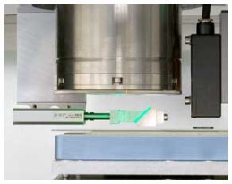
IGBT's are processed on thinned wafers. Often these thinned wafers are mechanically stabilized by using the so-called TAIKO grinding process (DISCO Corp., Japan) and a protection tape on the already processed front side. This tape is not compatible with high process temperatures. A high activation rate is achieved while the protection tape stays intact if the activation is performed with the VOLCANO® semi IGBT Laser Optics.
The backside illuminated CMOS image sensors require to activate a shallow pn junction at the surface of the wafer. Metal contacts are buried in the wafer at a depth of several µm, which are damaged by the high activation temperature. With the VOLCANO® semi IMAGE SENSOR Laser Optics it is possible to control the process precisely to limit the high process temperature to a shallow surface layer.
Laser Optics for Semiconductor Doping Activation |  Scientific Paper Dr. P. Oesterlin | ||||